Why 45- to 130-nanometer process nodes matter
Today, billions of transistors can be designed on a single chip. The more densely packed the transistors, the smaller the process node required. Some manufacturing processes use nodes as small as 5 nanometers (nm) and below.
However, foundational analog and embedded semiconductors produced in the 45nm to 130nm node range are ubiquitous in most of the electronics we use every day.
“In almost every electronic system, from automobiles and industrial applications to notebook computers and phone circuit boards, you see a wide ecosystem of semiconductors, most of which do not and will not need to use the smallest geometries,” said Hagop Kozanian, senior vice president, Analog Signal Chain at our company. “Most have an optimal performance using process technologies of 45nm nodes and above. In many designs for analog parts, just reducing node size can both degrade performance and increase price.”
The right tools for the job
Analog signal chain and power components don’t benefit from a race to the tiniest node. Instead, delivering the best part to market means designing and manufacturing with the methods and technologies that suit each part’s particular need.
“You need all sorts of specialized chips in the semiconductor industry to meet various application requirements. For most chip needs, node size is superficial,” Hagop said. “Our investments in 45nm-130nm process technologies help us deliver high precision at higher voltages, and that leads to better performance for applications like signals for radar systems and space satellites, and the ability to pack much more power into high-performance servers.”
The relationship between voltage and node size is complicated. Chips made at the smallest node sizes typically run on just a fraction of the voltage required even a few years ago. However, in analog sensor parts, for example, lower voltages mean that more hardware is needed to convert the signals, potentially introducing error and delay.
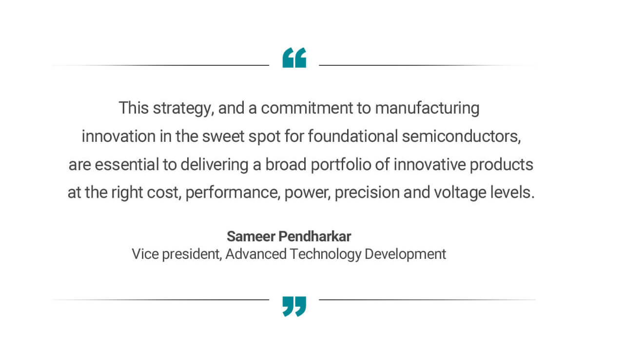
“In several industrial and automotive applications, we actually want to run on larger nodes, which support higher voltage devices. These devices help with efficient power delivery while reducing the total amount of copper wiring in the system,” said Sameer Pendharkar, vice president, Advanced Technology Development.
TI’s fully integrated microcontrollers with digital signal processing and radio capabilities are possible because of our investment in advanced 45nm node manufacturing, specifically for these types of products.

“Our process nodes are optimized for our products. On a typical TI microcontroller, wireless connectivity or radar device, over 60% of the die size is analog and RF optimized transistors. These transistors don’t shrink with the process node digital transistor geometry, and therefore do not provide any significant advantage with a smaller process node,” said Amichai Ron, senior vice president, Embedded Processing. “It would lead to a higher cost device with no performance benefits for our customers.”
Making investments that matter
Leadership in 45nm - 130nm process nodes requires development and ownership of process technologies uniquely suited for our products while also ensuring capacity is available when customers need it.
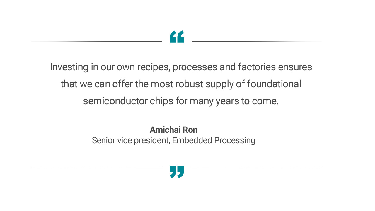
“In industries such as automotive and industrial, customers will need our products not just for a few years, but for decades,” Amichai said. “Investing in our own recipes, processes and factories ensures that we can offer the most robust supply of foundational semiconductor chips for many years to come.”
TI is one of the only semiconductor companies today growing 300mm investments in 45nm to 130nm manufacturing, and the only one that can internally support a full-product life cycle from design to delivery. Our investments include:
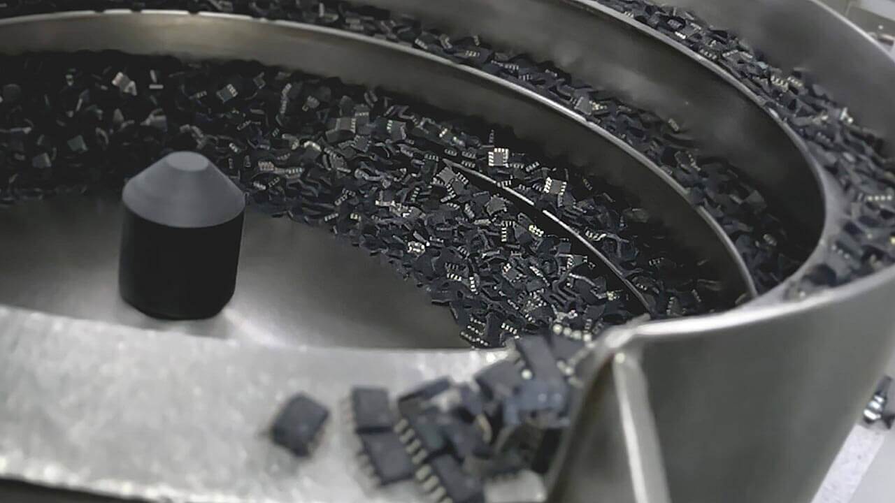
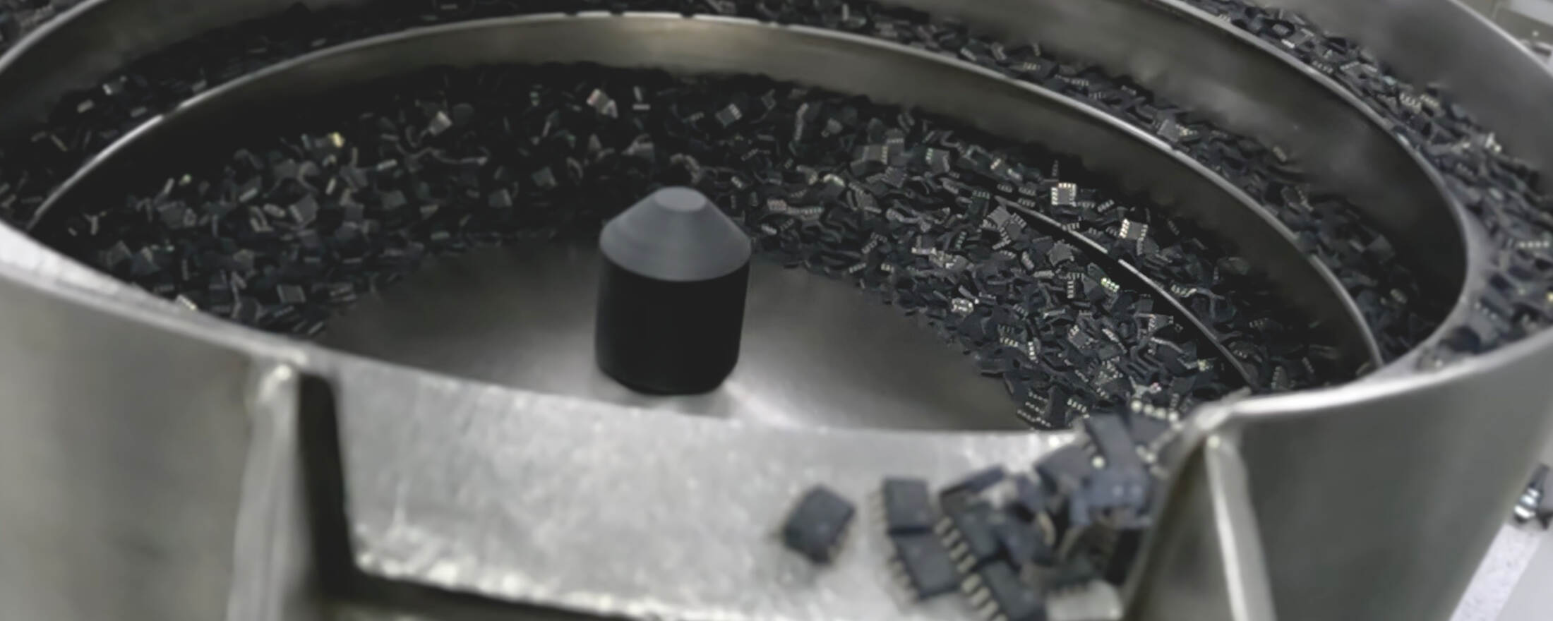
- Increased 300mm wafer capacity: Chips are first manufactured as circuits on large silicon wafers, and then they are cut into individual chips, assembled and packaged. Our recent investments in seven new 300mm wafer fabs will provide scale, efficiency and quality that support the continued growth of semiconductors in electronics for decades to come. The largest and most advanced size in the industry, 300mm wafers yield more than twice as many chips as 200mm wafers. So more 300mm wafer manufacturing means greater output with less energy and water usage per chip created, cost reductions and less overall waste.
- Optimal process technologies: Deeper investment in 300mm wafer manufacturing parallels our commitment to own our process technologies. Our recipes for 45nm-130nm process nodes are designed specifically for our products – ensuring that we can offer higher performance, better power density, lower power, smaller size and more – keeping the most innovative products available at the optimal intersection of price and performance.
- Increased assembly and test capacity: We also own and operate assembly and test facilities around the globe, giving us geographical diversity and control of the supply chain. We’re investing to grow our capacity and capability for assembly and test while also increasing availability of our manufacturing flows in multiple locations to provide reliable supply to our customers.
- Next-generation chip packaging: Unlike most semiconductor companies that ship their full wafer output volume to third parties, or outside assembly and test facilities (OSATs), for packaging into finished chips, we internally assemble the majority our products with thousands of standard and advanced package variations optimized for solution size, ease of use and performance.
“These investments secure our own supply and provide the right technologies for our products,” Sameer said. “And we are ready to grow into finer geometries as the market needs arise.”
Ensuring supply to a growing, thriving industry
We are making investments to bring more than 90% of our wafer manufacturing and assembly and test operations internal by 2030. By owning and operating our manufacturing facilities, we are able to better control our supply chain and offer a greater assurance of supply for our customers around the world.
“This strategy, and a commitment to manufacturing innovation in the sweet spot for foundational semiconductors, are essential to delivering a broad portfolio of innovative products at the right cost, performance, power, precision and voltage levels,” Sameer said.