The packages that encapsulate and protect integrated circuits have become increasingly critical as electronics get smaller and more components are integrated.

Our unique combination of research-and-development expertise in packaging, product design, technology development and manufacturing enables our customers to differentiate their products with smaller and more highly integrated chips that enhance reliability, increase performance and make electronics more affordable.
In applications ranging from medical electronics to factory automation, innovations in an increasingly important technology – semiconductor packaging – are helping meet demands for smaller, faster and more reliable chips that deliver high performance, improved power efficiency and lower costs.
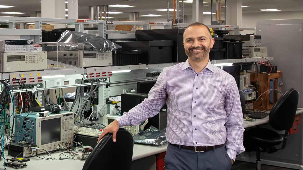
“Packaging is the bridge that enables electronic circuits to interact with the real world,” said Anindya Poddar, director of research and development for our company’s Packaging group. “Whether you’re watching your flat-screen television, listening to your smart earbuds, appreciating the efficiency of machines in an automated factory or riding in an autonomous vehicle, the things we enjoy are enabled through the miniaturization and integration of packaging.”
Semiconductor packages encapsulate digital circuits and connect them to circuit boards where they interact with other system components. There are thousands of package types.
Electronics are all around us, and mechanical systems are increasingly being replaced by electronics.
“Each type of electronic device has a different need,” said Sreenivasan Koduri, a TI Fellow who works on packaging technologies. “Chips used in outer space have much different requirements than a robot in a factory, servers in a data center or your phone, washing machine or electric vehicle. One size doesn’t fit all.”
The innovation required to design, develop and manufacture such a wide range of packages requires a unique set of capabilities.
Our company’s in-house research-and-development expertise across packaging, product design, technology development and manufacturing provide a unique advantage to optimize packaging technology.
Miniaturization
Before Jack Kilby invented the integrated circuit in 1958, electronics were packaged in glass or metal tubes because those materials could withstand the high levels of heat the circuits generated. In the decades since Jack’s breakthrough, semiconductors have become ubiquitous as each generation became more affordable and allowed them to go into electronics everywhere. But with the focus on the capabilities of the circuits, the plastic packages that enclosed them became an afterthought.
No more. Packaging is increasingly important as a differentiator in semiconductors because of the benefits it delivers. Packaging decisions are made at the initial design stages to ensure that devices meet design engineers’ size, power density, performance and reliability needs.
Today, designers seek smaller packages that are capable of handling higher power while still protecting their delicate circuits. Some of the industry’s smallest integrated circuits are helping engineers create smaller and smaller designs, such as tiny wearable electronics used in patient monitoring applications, miniature microphones used in voice- or speech-based systems, and tiny earbuds enabled by ultra-small temperature sensors.

A typical package includes the integrated circuit and wires that connect it to leads, which connect the package to a printed circuit board.
Today, we supply the industry’s smallest operational amplifier, which measures less than one square millimeter, along with the smallest digital temperature sensor, Ethernet PHY transceiver and isolated CAN transceiver – just to name a few. Packaging innovations from our company enable integrated circuits such as these – some smaller than a speck of pepper. Our tiny products allow designers to reduce overall solution size – and often cost – or provide more features in the same amount of space without sacrificing performance and reliability.
“The challenge with miniaturization is increasing power density in smaller spaces,” Anindya said. “Packaging is crucial for managing higher thermal requirements so that our customers’ products can be used safely, reliably and repeatedly in all kinds of electronic products.”
Integration
Enclosing more than one chip – as well as components such as inductors, capacitors, isolation barriers and sensors – in a single package can shrink the overall component size, reduce system cost, improve circuit speed and efficiency, and increase system reliability.
“Integrating these devices allows designers to do a lot more things that aren’t possible when you have one circuit in a package,” Sreenivasan said. “Integration – enabled by packaging – has opened up a new world.”
In the automotive market, for example, the industry’s first automotive-qualified gallium nitride (GaN) device to power on-board charging systems in electric vehicles integrates a GaN-on-silicon field effect transistor (FET) and a fast-switching silicon gate driver to give customers an easy way to integrate a switch, controller and protection technologies onto a single chip with a thermally enhanced package so that the solution can withstand higher voltages. Our company’s GaN-on-silicon substrate leverages processing capabilities to provide a cost advantage over comparable substrate materials such as silicon carbide.

To help design engineers support the increasing number of power domains in industrial communications applications, a four-channel digital isolator from our company integrates a chip-scale transformer, enabling signal and power isolation in a single, small form-factor package. In addition to reducing board space by 30% compared to discrete signal and power isolation solutions, this level of integration increases system performance and simplifies system certification through industry-low radiated emissions, which is key for applications in harsh industrial environments.
Our latest millimeter wave technology directly integrates the antenna onto the package, making development more affordable and providing the advantage of an extremely small form factor to enable flexible sensor placement in new locations, such as a door handle. Our millimeter wave innovation provides system-on-a-chip radar technology to enable 3D object detection around the vehicle, in-cabin occupant detection and brings safety features to a broad range of automobiles.
Improving specifications
The line between chip design and package design – once two distinct processes – has become nonexistent as the importance of chip packaging has increased.
“The package used to be a passive component that enabled the circuit, but its role has changed over time,” Sreenivasan said. “Now, the package in many cases is not only supporting, encapsulating and protecting the die, but is itself enabling the functionality. Packaging is improving the specifications of the device.”
And miniature, integrated packages will continue to improve how we live, learn and work.
“Packaging puts more functionality into smaller spaces and gives people who use our products more value,” Anindya said. “Integration and miniaturization – together with manufacturing excellence – create opportunities for innovation while making electronics more affordable for everyone.”
Living our passion to create a better world
Helping our customers design and produce smaller, faster, more reliable products that offer high performance, improved power efficiency and lower costs is one example of how TI innovators are living our company’s passion to create a better world by making electronics more affordable through semiconductors. As each generation of innovation builds upon the last to make technology smaller, more efficient, more reliable and more affordable, new markets open and it becomes possible for semiconductors to go into electronics everywhere. At TI, we think of this as Engineering Progress. It’s what we do and have been doing for decades.